“Dam and fill” is a technique used in electronics manufacturing and semiconductor packaging to address the challenges of encapsulating delicate components with epoxy resin or other encapsulant materials.
In certain electronic devices, there might be components that are placed relatively close to each other on a circuit board or within a semiconductor package. These components can generate heat during operation, and the thermal expansion and contraction rates of different materials might not match perfectly. This can result in mechanical stress and the potential for solder joint failures or other reliability issues.
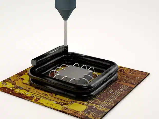
The “dam and fill” process involves creating a physical barrier (the “dam”) around a component before applying the encapsulant (the “fill”). The dam prevents the encapsulant from flowing to unwanted areas, directing it to cover the intended region more precisely. This technique is particularly useful when there are small gaps or spaces between components that need to be filled with epoxy or another encapsulant material.
Here’s a basic overview of the process:
1. Dam Formation: A dam material, often a specially formulated epoxy, is dispensed or applied around the edges of the component that requires encapsulation. This dam material is designed to stay in place and prevent the encapsulant from spreading beyond the designated area.
2. Encapsulant Dispensing: The encapsulant material, typically an epoxy resin, is then dispensed within the area defined by the dam. This encapsulant will fill the gaps and spaces around the component, providing mechanical support and improving thermal performance.
3. Curing: The entire assembly, including the dam and encapsulant, is cured according to the manufacturer’s specifications. Curing involves allowing the epoxy or encapsulant material to harden and solidify, creating a durable and stable protective layer around the component.
The “dam and fill” technique helps ensure that the encapsulant material is precisely placed, reducing the risk of short circuits, electrical interference, and mechanical stress. This is particularly important in advanced electronics manufacturing where components are becoming smaller and more densely packed. The technique contributes to the overall reliability and performance of electronic devices.